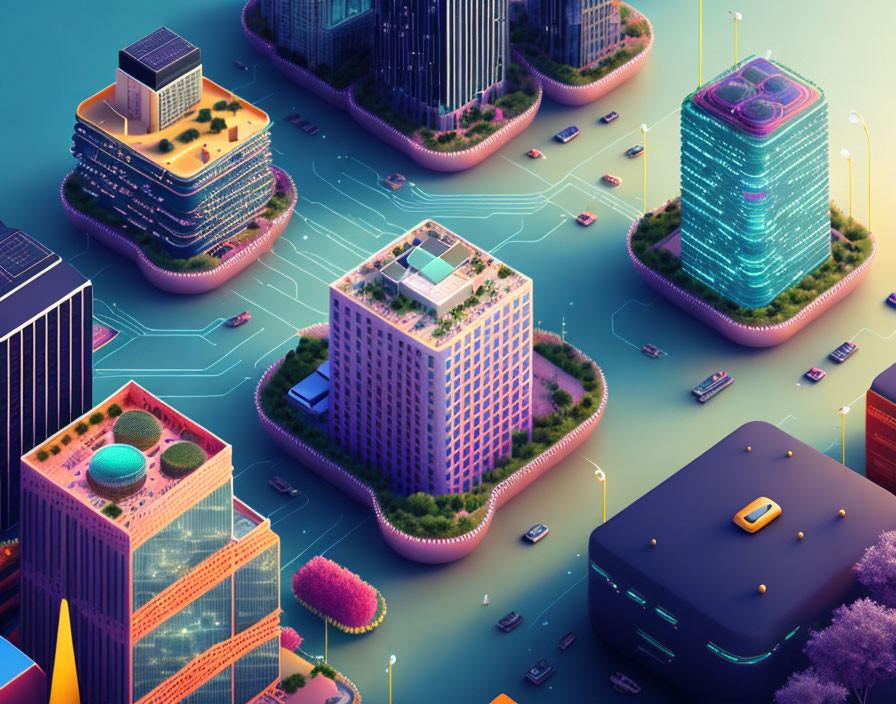
Graphene catches terahertz light with bouncing plasmons in a nanoscale cavity

A new study published in ACS Photonics, led by SUPERVenice researcher Domenico De Fazio, shows that scalable graphene can host coherent acoustic plasmon resonances and use them to enhance terahertz detection. Terahertz radiation sits between microwaves and infrared light in the electromagnetic spectrum. It can pass through many common materials, interact with molecular vibrations, and carry information at high frequency, making it promising for imaging, sensing, security screening, and future wireless communications. Yet detecting terahertz light efficiently, especially in compact devices, remains a major technological challenge. This study reports an advance in this direction using one of the thinnest possible materials: graphene. It demonstrates that chemical-vapor-deposited graphene — a scalable form of graphene compatible with larger-area fabrication — can support coherent acoustic plasmon resonances at terahertz frequencies under the right conditions. In simple terms, the researchers show that tiny waves of charge in graphene can be made to bounce back and forth inside a microscopic cavity, producing a measurable enhancement in the terahertz photoresponse. Turning graphene into a tiny terahertz resonator Graphene is only one atom thick, but its electrons can respond strongly to electromagnetic radiation. When terahertz light hits a graphene device, it can heat the electrons and generate a voltage through the photothermoelectric effect. This makes graphene attractive for terahertz photodetectors. However, because graphene is atomically thin, it normally absorbs only a small fraction of incoming light. To overcome this limitation, the team designed a device in which the metallic gates also act as a terahertz antenna. These gates concentrate the incoming terahertz field into the graphene channel and launch acoustic graphene plasmons — collective oscillations of electrons coupled to the electromagnetic field. At cryogenic temperatures, where electronic losses are strongly reduced, these plasmons become coherent enough to form standing waves. “By cooling the device down, the system becomes quiet enough for us to see the plasmons bouncing back and forth inside the graphene cavity,” explains De Fazio. “It is a bit like watching waves resonate in a tiny box, except that here the box is a graphene channel only a few micrometres long, and the waves are charge oscillations driven by terahertz light.” A full cavity — or only half of it One of the key results of the study is that the plasmon cavity can be reconfigured electrically. By changing the voltages applied to the two gates, the researchers can modify the carrier density profile inside the graphene channel. In one configuration, the plasmon resonance extends across the full graphene channel. In another, the device behaves as if only half of the channel forms the resonant cavity. This “half-cavity” behaviour occurs because the gate-defined conductivity landscape creates an internal reflection point for the plasmons. This gate-controlled behaviour gives direct evidence that the observed peaks in the terahertz photoresponse arise from acoustic plasmon Fabry–Pérot-like cavity modes, rather than from a simple background heating effect. The paper reports that the resonances modulate the photothermoelectric response by up to about 40% at low temperature, with the modes disappearing as the device is warmed due to increased plasmon damping. Why this matters The result is important because it shows that coherent acoustic plasmon cavity modes are not limited to the highest-quality exfoliated graphene devices. Here, the team uses CVD graphene, a form of graphene that is more suitable for scalable fabrication. This opens a route toward compact, frequency-selective terahertz detectors based on engineered graphene cavities. Such devices could eventually contribute to terahertz imaging, spectroscopy, on-chip sensing, and next-generation communication technologies. The work also highlights the broader potential of polaritonic engineering: instead of detecting terahertz light only through direct absorption, the device uses strongly confined light–matter waves to concentrate energy into nanoscale regions and convert it into an electrical signal. Collaboration and visualisation The study was carried out by an international team including researchers from Ca’ Foscari University of Venice, ICFO, the University of Ioannina, Queen Mary University of London, the University of Manchester, INMA-CSIC/University of Zaragoza and other collaborators. The visual concept accompanying the work was created by David Alcaraz Iranzo, who represented the acoustic plasmons as colourful waves bouncing through a graphene cavity, helping translate a highly nanoscale physical process into an intuitive image. For SUPERVenice, the publication reflects the hub’s mission to connect advanced materials, photonics and emerging device concepts, bringing fundamental discoveries closer to future technologies. The full article can be found at the following link: https://pubs.acs.org/doi/10.1021/acsphotonics.6c00272

Graphene catches terahertz light with bouncing plasmons in a nanoscale cavity Read More »

Telecommunication-inspired network models of healthy and diseased brains

The article recently published by Prof. Peppino Fazio, a member of the SUPERVenice team, and co-authors, presents a detailed analysis of functional connectivity in the human brain modeled upon the paradigm of telecommunication. Each brain region is seen as a transmitter and receiver, and the signal travels through functional pathways between brain regions. In particular, the authors consider a discrete finite-state model to map the behavior of neurons within a neuronal agglomerate, and investigate of the effect of disruption provoked by the presence of a disease. The authors complete the analysis with real data from healthy brains and brains of patients affected by Alzheimer’s disease. Recent advances in nanoelectronics have spurred increased interest in the human brain and its complex functions. Numerous studies have explored brain behavior in varying levels of detail, from individual neurons to entire lobes. Intricately structured, the brain is a complex organ susceptible to diseases that may disrupt the connectivity between its internal regions. Investigating this phenomenon, the present study applies a discrete finite-state model to map the behavior of neurons within a neuronal agglomerate and examine of the effect of disease on these behaviors. Each agglomerate is then compared to a wireless clustered network and modeled as a finite-state system, with inter-cluster communications analyzed under conditions of temporal variations and degradation. This work represents one of the most advanced applications of discrete finite-state processes and routing theory in brain modeling. The work of Prof. Fazio and co-authors addresses, in a cutting-edge and interdisciplinary way, a challenging problem, that is, the analysis of brain-network alterations occurring in presence of a neurodegenerative disease with high social impact such as Alzheimer’s disease. The methods are fully inspired by physics of complex networks and are mostly derived from computer engineering and telecommunication engineering, and they are applied to a problem of neurology. The attention is mainly focused on whole-brain analysis and signal exchange between brain regions. The method can be applied independently from the choice of the specific brain atlas. The full article can be found at this link: https://www.nature.com/articles/s41598-026-50758-x

Telecommunication-inspired network models of healthy and diseased brains Read More »

Superconductivity gets a Boost from Nanoscale Substrate Design

A new international study involving Ca’ Foscari University of Venice, carried out in close collaboration with Chalmers University of Technology (Göteborg, Sweden) and other research partners, has identified a powerful new way to strengthen superconductivity in ultrathin copper-oxide films. The work shows that the nanoscale morphology of the substrate on which a superconducting film is grown can actively enhance its properties, leading to a higher superconducting onset temperature and a much stronger resistance to applied magnetic fields. The study, published in Nature Communications, focuses on YBa2Cu3O7-δ (YBCO), one of the most extensively studied high-temperature cuprate superconductors. By combining transport measurements, spectroscopy, structural and morphological characterization, and theoretical modelling, the researchers demonstrate that the interface between the film and the substrate can be engineered as an effective tool to manipulate the electronic ground state of the material.   A new route to control cuprate superconductors Unlike many two-dimensional materials, cuprates cannot be easily tuned after growth. Their carrier density is largely fixed during synthesis, and conventional electrostatic gating is generally ineffective. For this reason, finding alternative ways to control their properties remains a central challenge in the field. In this work, the researchers show that one such route lies in the substrate itself. Before film deposition, the surface of (110)-oriented MgO is thermally reconstructed, producing a quasi-periodic landscape of nanofacets with ridges and valleys on the nanometer scale. When YBCO is grown on this textured surface, the interface induces an additional electronic potential that has a profound impact on the superconducting state.   Stronger superconductivity in ultrathin films The most remarkable effects emerge in the thinnest films. Compared with 50 nm samples, 10 nm YBCO films grown on the nanofaceted substrate display a superconducting onset temperature more than 15 K higher and an upper critical field enhanced by more than 50 tesla. For Riccardo Arpaia, researcher at Ca’ Foscari, the result is especially meaningful because it builds on a materials platform that has been studied for many years: “These YBCO films on MgO have been part of our research journey since the very beginning of my PhD, around fifteen years ago, and they have never stopped surprising us. But this result goes beyond expectations: seeing a critical temperature higher than in the bulk material, and understanding that this originates from the growth dynamics we induced at the interface, shows that we can genuinely learn to manipulate materials in increasingly precise ways to obtain stronger superconducting properties.”   When the substrate becomes an active element According to the combined experimental and theoretical analysis, the enhancement is linked to the emergence of an interfacial electronic order involving electronic nematicity and unidirectional charge density waves, both promoted by the specific nanoscale texture of the substrate. Rather than acting as a passive support, the substrate becomes an active element that reshapes the electronic landscape of the film and stabilizes stronger superconductivity. This is one of the most significant aspects of the study: it suggests that the performance of complex quantum materials may be improved not only through chemistry, but also through the deliberate design of interfaces and surface morphology.   A broader perspective for quantum materials research For Ca’ Foscari, the study highlights the importance of international and interdisciplinary research on superconductivity and quantum materials, as well as the value of long-term collaborations capable of integrating materials growth, advanced characterization and theory. More broadly, the findings point to a new paradigm for superconductor design. Instead of improving performance only by modifying composition, it may be possible to enhance superconducting properties by tailoring the substrate and the interface at the nanoscale. This opens promising perspectives for future high-performance superconducting materials for energy-efficient electronics, high-field magnet technologies and quantum devices.   The full study is published in Nature Communications and is available at https://doi.org/10.1038/s41467-025-67500-2

Superconductivity gets a Boost from Nanoscale Substrate Design Read More »

Skin-safe, flexible photodetectors combine graphene and carbon dots for wearable sensing

Researchers from Ca’ Foscari University of Venice, working within the SUPERVenice research unit, have developed a new type of flexible, skin-compatible photodetector that can sense light across a broad range of wavelengths while operating at low voltage and remaining safe for direct contact with human skin. The device, reported in Advanced Functional Materials, combines graphene with specially engineered carbon dots on a plastic substrate, creating a lightweight and bendable photodetector suitable for wearable electronics and on-skin sensing applications. Addressing a key challenge in wearable optoelectronics Photodetectors—devices that convert light into electrical signals—are essential components in technologies ranging from cameras and optical communications to medical sensors. Conventional photodetectors, often based on rigid silicon electronics, perform well but are poorly suited for wearable or skin-integrated systems, where flexibility, low power consumption and biocompatibility are crucial. Many flexible photodetectors reported to date compromise on at least one of these requirements. Some offer high sensitivity but rely on toxic materials such as lead- or cadmium-based quantum dots; others are flexible but operate over a narrow spectral range or lack evidence of skin safety. The new work addresses these limitations by combining broadband optical response, mechanical flexibility and verified skin compatibility within a single device architecture. Carbon dots and graphene: complementary roles The photodetector is built by integrating hydrothermally synthesized carbon dots with single-layer graphene transferred onto a polyethylene terephthalate (PET) substrate. The carbon dots act as the light-absorbing element, while graphene provides an efficient, high-mobility pathway for charge transport. Unlike conventional quantum dots, the carbon dots used in this study are metal-free, environmentally benign and inherently biocompatible. By carefully tuning their synthesis conditions, the researchers engineered the dots to absorb light not only in the ultraviolet but also across the visible and near-infrared range, extending roughly from 400 to 800 nanometers. Graphene alone absorbs only a small fraction of incoming light, but when coupled to the carbon dots it efficiently collects photogenerated charge carriers, enabling a measurable electrical response across the full spectral window. Low-voltage operation with a biopolymer gate To control the device electronically, the team used a chitosan–glycerol biopolymer electrolyte as a gate dielectric. Chitosan, derived from natural sources such as chitin, is non-toxic and widely used in biomedical applications. This electrolyte enables strong electrostatic gating at very low operating voltages, with optimal performance reached at around 0.5 V, well below the levels typically required by flexible photodetectors. Under illumination, the device shows a gate-dependent photoresponse that can be tuned between different operating regimes, with peak responsivities of approximately 0.19 A/W at 406 nm, 0.32 A/W at 642 nm, and 0.18 A/W at 785 nm. Performance under bending and repeated use Mechanical flexibility is a key requirement for wearable electronics, and the researchers subjected their devices to extensive bending tests. The photodetectors maintained stable operation at bending radii as small as 0.8 cm and showed no significant degradation after up to 1000 bending cycles. The response times, on the order of one second, are compatible with many wearable sensing applications, including biometric monitoring and environmental light sensing. Demonstrated skin compatibility Beyond electrical and mechanical performance, the study directly addresses skin safety, an aspect often assumed rather than tested in wearable optoelectronics. Using reconstructed human epidermis models and fibroblast cultures, the researchers showed that neither the complete device nor its individual components caused skin irritation or cytotoxic effects. Importantly, illumination under realistic operating conditions did not induce detectable reactive oxygen species (ROS) generation, indicating that the device is photo-safe for on-skin use. Toward practical wearable photonics While the device is presented as a proof of concept, the authors emphasize that the materials and fabrication steps are compatible with scalable, low-cost processing. Future work will focus on improving detectivity, optimizing large-area uniformity, and integrating the photodetectors into functional wearable platforms. By combining metal-free light absorbers, graphene electronics, biopolymer gating and direct biological testing, the study outlines a practical route toward next-generation photodetectors designed from the outset for safe, wearable operation. The full study is published in Advanced Functional Materials and is available at https://doi.org/10.1002/adfm.202523076

Skin-safe, flexible photodetectors combine graphene and carbon dots for wearable sensing Read More »

Simulations Point the Way to Next-Generation SiC Power Packaging

A new study led by researchers at Ca’ Foscari University of Venice, in collaboration with ON Semiconductor, University of Naples Federico II, and University of Applied Sciences Kempten, has unveiled a powerful digital approach to designing the future of high-efficiency power electronics. The work, recently accepted for publication in the IEEE Open Journal of Power Electronics, is titled “Multi-Physics Simulations of a 1.2 kV Embedded SiC Prepackage”. The research team includes Saimir Frroku, Ankit Bhushan Sharma, Pierfrancesco Fadini, Klaus Neumaier, Andrea Irace, Till Huesgen, and Giovanni A. Salvatore, who coordinated the study at Ca’ Foscari’s Department of Molecular Sciences and Nanosystems. A New Era for Power Device Packaging Wide-bandgap (WBG) semiconductors such as silicon carbide (SiC) are transforming power electronics thanks to their ability to operate at higher voltages, temperatures, and switching frequencies than traditional silicon. Yet, packaging remains a critical bottleneck—how these chips are physically mounted, cooled, and electrically connected determines the true performance and reliability of a power module. Embedding the SiC chips directly into an insulating substrate represents a breakthrough approach. By eliminating bulky wire bonds and reducing parasitic inductances, embedded packages enable faster and cleaner switching, boosting efficiency and compactness. However, questions of mechanical reliability and heat management have persisted. Digital Twins for Real-World Reliability The Ca’ Foscari team tackled these challenges through multi-physics finite-element simulations, virtually reconstructing a “prepackage” containing two 1.2 kV SiC MOSFETs and exploring different commercial substrates—alumina, silicon nitride, aluminum nitride, and insulated metal boards (IMS). Their thermomechanical “digital twin” captured how heat and mechanical stress propagate during manufacturing and operation, allowing the team to pinpoint design weaknesses long before physical prototyping. Using a Pareto-based optimization, they identified aluminum nitride (AlN) as the most balanced substrate, achieving a thermal resistance of just 0.27 K/W and low mechanical strain levels. Engineering Smarter Structures The simulations also revealed how to strengthen the package against long-term mechanical fatigue. Replacing the traditional solid copper top contact with a pillar-like interconnect geometry reduced creep strain in the silver sintering layer by up to fourfold—a major leap for reliability. Even the cooling rate during manufacturing proved to be a critical factor: above a certain threshold (around 40 K/min), creep deformation virtually disappears, leaving only reversible plastic strain. This insight offers a new lever for process control and reliability enhancement. Toward Scalable, High-Frequency Power Modules By virtually paralleling four optimized prepackages, the researchers demonstrated a compact power module with only 3 nH of stray inductance, suitable for high-frequency, high-efficiency power conversion—crucial for electric vehicles, renewable-energy systems, and data-center power supplies. “These simulations allow us to accelerate innovation while reducing costly trial-and-error fabrication,” explains Giovanni A. Salvatore, senior author of the study. “Digital modeling provides predictive insights into reliability and performance, helping us design the next generation of power modules that are both efficient and robust.” From Simulation to Sustainable Energy Systems The findings open new perspectives for integrating wide-bandgap semiconductors into compact, thermally stable, and manufacturable modules—an essential step toward electrified mobility and renewable-powered grids. The team’s work exemplifies how virtual engineering and experimental design can converge to drive sustainable innovation in advanced electronics. The full article is available at: https://ieeexplore.ieee.org/document/11224018. All image rights and copyrights are reserved by IEEE.

Simulations Point the Way to Next-Generation SiC Power Packaging Read More »

From Biowaste to Green Electronics: Pioneering Biobased Piezoelectric Films

A team of researchers at the Ca’ Foscari University of Venice has developed a new class of sustainable, flexible, and biodegradable materials that could transform the future of wearable technologies, robotics, and green electronics. The study, published in ACS Nano and featured on its supplementary cover, demonstrates how chitosan-based thin films—derived from crustacean biowaste—can be engineered to achieve record piezoelectric performance. Turning waste into innovation Chitosan, a natural polymer obtained from chitin in crustacean shells, is already known for its biocompatibility and biodegradability. By incorporating chitin nanocrystals into chitosan films, the Ca’ Foscari-led team achieved a twofold increase in piezoelectric response. These soft, transparent films are also stretchable up to 40% strain and exhibit a low Young’s modulus (~100 MPa), closely mimicking the elasticity of human tissues. Why it matters Piezoelectric materials are the backbone of sensors, actuators, and energy harvesters. Today, most commercial devices rely on synthetic polymers like PVDF or inorganic ceramics such as PZT, which raise environmental and health concerns due to their toxicity, rigidity, or reliance on fluorinated compounds. The Ca’ Foscari study shows that biobased materials can achieve competitive performance without compromising sustainability. The films are fully biodegradable, scalable in production, and derived from low-cost biowaste—an example of circular economy applied to advanced materials science. Potential applications Because of their softness and biocompatibility, the new chitosan nanocomposites are particularly suited for: A collaborative effort The research was carried out by the LION group (Laboratory for Innovation in Organic and Nanostructured materials) at Ca’ Foscari’s Department of Molecular Sciences and Nanosystems, in collaboration with international partners. The project received support from EU NextGenerationEU programs (PRIN 2022, iNEST ecosystem) and the PRIMA initiative for sustainable bio-based packaging. Looking ahead According to Giovanni Antonio Salvatore, corresponding author of the study, this work “opens the door to a new generation of sustainable-by-design materials for electronics, capable of replacing polluting polymers and bridging the gap between biological systems and technology.” With this breakthrough, Ca’ Foscari University of Venice further strengthens its position at the intersection of materials science, sustainability, and technological innovation. 👉 Read the full article in ACS Nano: https://doi.org/10.1021/acsnano.4c12855

From Biowaste to Green Electronics: Pioneering Biobased Piezoelectric Films Read More »

Venice shines bright for the FISMAT 2025 conference

From July 6 to 11, 2025, the historic San Giobbe Economics Campus of Ca’ Foscari University welcomed over 1,100 attendees from across the globe for FISMAT 2025, a landmark gathering on the “physics of matter” (eventi.cnism.it). The state‑of‑the‑art venue—with its 23,000 m² dedicated to research, teaching, and relaxation in its lush 2,000 m² garden—offered the perfect backdrop for a conference that exceeded all expectations. The event featured a robust program of invited talks, contributed sessions, and stimulating workshops, including a spotlight on the ISOL technique for medical radionuclide production (LinkedIn). Prominent scientists from institutions like EPFL, Max Planck, Università di Milano, and the Goethe Universität gathered in the Cannaregio district to present cutting-edge research, network, and forge collaborations. Figures of Merit: Attendance: Over 1,100 participants—well beyond initial estimates Speakers: A stellar international lineup, spanning physics, math, and engineering Venue: Conveniently located near Santa Lucia station and Piazzale Roma, with excellent water‑bus connections A Night to Remember: Dinner at Palazzo Moro On Wednesday evening, attendees gathered at the opulent Palazzo Moro, an elegant 16th-century palace nestled in the Cannaregio district. Built by the Moro-Bizio family, this Venetian gem is renowned for its Renaissance façades and frescoed interiors. The palace provided a magical setting for the conference dinner, where guests enjoyed fine Venetian cuisine and heartfelt conversations under shimmering chandeliers. Against the backdrop of historic frescoes, colleagues deepened connections over prosecco, seafood risotto, and local desserts—truly a Venetian feast. What’s Next? With such resounding success, FISMAT 2025 has firmly positioned Venice as a hub for high‑caliber scientific exchange. Attendees departed inspired, carrying with them both fresh insights and unforgettable memories of our city’s magic.   📸 Sneak Peeks from FISMAT 2025 📸 Thank you to everyone—organizers, speakers, sponsors, and attendees—who helped make FISMAT 2025 a shining success. Venice awaits even more groundbreaking discoveries next time!  

Venice shines bright for the FISMAT 2025 conference Read More »

“p-Wave” Magnetism: A Unique Behavior of Electrons

A team led by the Massachusetts Institute of Technology, with the participation of SuperVenice, has recently reported a new form of magnetism, called p-wave, in the material NiI₂. This material exhibits a very peculiar internal magnetic structure: the magnetic moments of the atoms — essentially tiny atomic compasses — are arranged in a spiral pattern. One consequence of this structure is that electrons behave in a unique way: their spins are tied to their energy and direction of motion according to a symmetry known as p-wave. In practice, if an electron reverses its direction of motion, its spin also flips, following precise rules. Furthermore, as demonstrated experimentally, in NiI₂ this property can be controlled electrically, without the need for magnetic fields, which are usually required to manipulate spins.Why it matters Although this type of magnetism in NiI₂ appears only at low temperatures, its potential observation in materials stable at room temperature could lead to the development of much faster and more efficient information processing devices compared to those currently available. The full article, published in the “Nature” journal, is available at the following link: https://www.nature.com/articles/s41586-025-09034-7

“p-Wave” Magnetism: A Unique Behavior of Electrons Read More »

Graphene Meets MoS₂: New Path to Control Light at the Nanoscale

In a study just published in ACS Nano, the team investigated what happens when monolayer MoS₂ — a direct-gap semiconductor just three atoms thick — is stacked with graphene. This combination of two-dimensional (2D) materials reveals a subtle but powerful mechanism: electrical control over light emission without relying on high levels of doping. By carefully tuning the interaction between MoS₂ and graphene, the researchers observed a dramatic suppression of photoluminescence (light emission) from specific exciton species (bound electron-hole pairs), depending on whether the material was isolated or part of a stacked heterostructure. The introduction of graphene changes the game: it enables efficient, voltage-controlled charge transfer, preventing the accumulation of excess carriers in MoS₂ and thus keeping the optical response stable and predictable. The most striking insight? In pristine MoS₂, high doping leads to a superlinear increase in light emission — a kind of optical “amplification” that stops once the system is saturated. This effect disappears completely in the MoS₂/graphene stack, showing that graphene acts as a natural “exciton regulator,” draining away excess charge and suppressing this nonlinearity. Even B-type excitons — typically unaffected by doping due to their ultrafast decay — are modulated by this setup, revealing that charge transfer occurs before excitons can recombine internally. This suggests the presence of a hot-electron transfer channel, a new dimension to 2D material photophysics. Why it matters This work opens the door to more precise control over how atomically thin materials emit light, essential for developing efficient LEDs, photodetectors, and quantum light sources. The use of layered 2D materials to achieve such control, without chemical treatment or structural modification, marks a significant leap forward in optoelectronics and nanophotonics. The SUPERVenice perspective This discovery strengthens Venice’s growing role in frontier materials research. The participation of Ca’ Foscari University through Prof. Domenico De Fazio, member of SUPERVenice, highlights the impact of collaborative, interdisciplinary science rooted in fundamental physics with clear technological implications. The full paper, “Tunable Exciton Modulation and Efficient Charge Transfer in MoS₂/Graphene van der Waals Heterostructures”, is available open-access in ACS Nano. 🔬 Read the paper: ACS Nano DOI

Graphene Meets MoS₂: New Path to Control Light at the Nanoscale Read More »

Securing the Future: A Review of Key Management in QKD Networks

Secure communication is essential to modern digital infrastructure, enabling safe data exchange across global telecommunication networks. As computational capabilities grow, so do threats to classical encryption, prompting the development of advanced cryptographic methods. Quantum Key Distribution (QKD) offers a groundbreaking solution by enabling information-theoretically secure (ITS) key exchange, rooted in the principles of quantum mechanics rather than computational hardness. Unlike traditional methods, QKD remains secure even against adversaries with unlimited processing power. To overcome the distance limitations of direct quantum communication, trusted relay QKD networks have been developed. These networks act as secure extensions to classical systems, facilitating the generation and distribution of cryptographic keys across larger scales. However, due to limited key generation rates, efficient key management is critical, especially when integrating QKD into critical infrastructures. Key management ensures optimal use of resources, addressing challenges like key allocation, storage, and prioritization. The accepted work addresses this need by providing a comprehensive review of key management approaches tailored for trusted-relay QKD networks. The surveyed strategies encompass various aspects of key lifecycle management, such as key generation, storage, routing, prioritization, and expiration, as well as integration with existing security protocols and infrastructure requirements. Through in-depth analysis, the paper aims to identify promising techniques, highlight existing limitations, and outline areas for further research. The ultimate goal is to facilitate the strategic development and deployment of scalable, secure, and efficient QKD networks that can be seamlessly integrated into existing communication infrastructures, paving the way for a quantum-safe future. The work is also the result of a long-term research cooperation between researchers from University of Sarajevo (Department of Telecommunications) Bosnia-Erzegovina, VSB-Technical University of Ostrava (Department of Telecommunications) Czech Republic and Ca’ Foscari University of Venice (Department of Molecular Sciences and Nanosystems) Italy. The full article is available at the following link: https://dl.acm.org/doi/10.1145/3730575

Securing the Future: A Review of Key Management in QKD Networks Read More »