Micro/Nano-Fabrication Lab
Responsible: Domenico De Fazio
Instruments and tools:
- Laser writer Microtech LW405-E (~400 nm resolution)
- Reactive ion etching Moorfield nanoETCH
- e-Beam evaporator Kenosistec KE400E+load lock
- Plasma asher Diener Zepto-BLS
Electronics Lab
Responsible: Giovanni A. Salvatore
Instruments and tools:
- Probe station FormFactor EPS150TRIAX-EDU
- Keysight B1500A semiconductor parameter analyzer
- SR860 lock-in amplifier, dual channel Keysight B2902B source meter, waveform generators, oscilloscopes, virtual network analyzer, bench power supplies, cDAQ bundle + chassis, USRP transmitters, LCR meter, and digital multimeters
- Thorlabs MCLS1-custom 4-channel laser source (406 nm, 642 nm, 785 nm, 1550 nm, all Fabry-Perot)
- Stretching set-up
- Deben microtest three point bending setup
- 3D printer, dispenser, analytic scales, film applicator, benchtop programmable mechanical cutter plotter
- Zeiss stereo-microscope
- HQ graphene microscope + transfer system for 2D material heterostructure assembly
- Fume hood, hot plates, and soldering station
Laser Optics Lab
Responsible: Enrico Trave
Instruments and tools:
- Renishaw inVia confocal Raman spectrometer with three laser wavelengths (514 nm, 633 nm, and 785 nm), three gratings (1200 l/mm, 1800 l/mm, and 2400 l/mm) + Linkam thermal stage
- CI Systems SR-800N extended area blackbody source
- Terahertz time-domain spectroscopy setup
- Spectrofluorometer
- Q-switched Nd:YAG laser + Optical parametric oscillator (OPO)
- 8 W Ar-Kr continuous-wave (CW) laser multiline
Sputtering Lab
Responsible: Elti Cattaruzza
Instruments and tools:
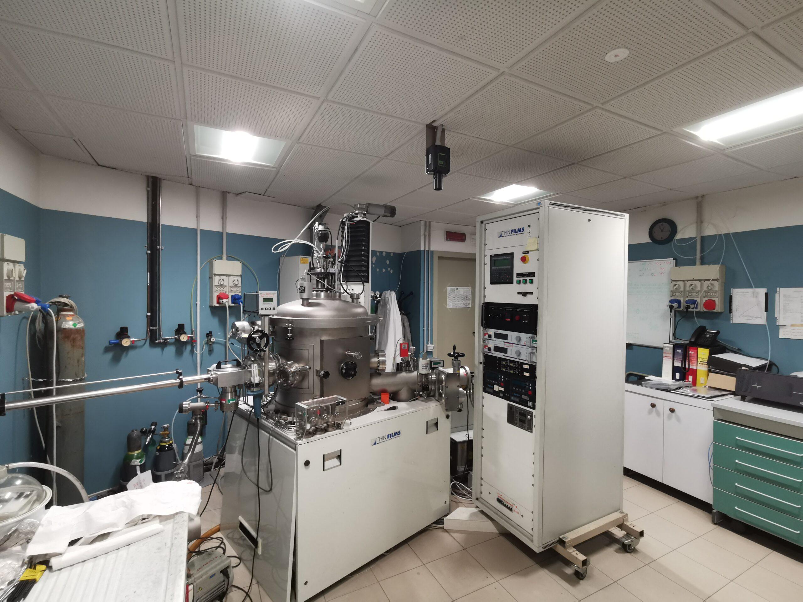
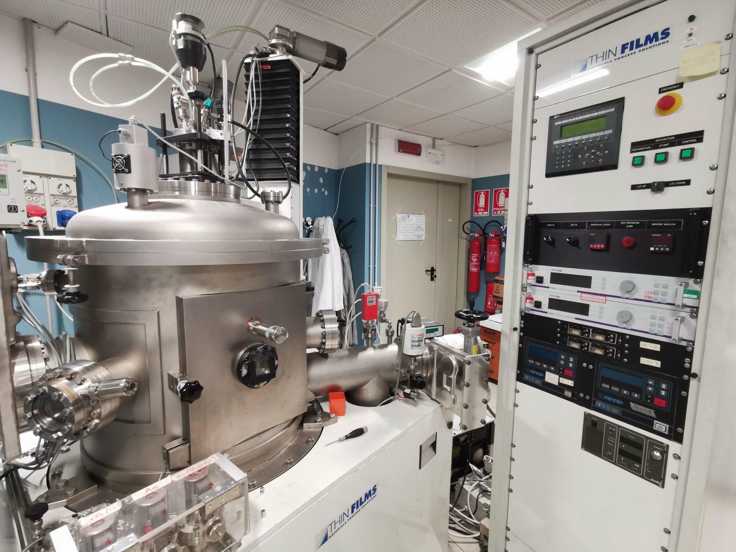
- Custom-built RF-magnetron sputtering system for thin films deposition, equipped with three independent circular (2 inches diameter), water-cooled, planar radiofrequency (13.56 MHz) magnetron sources. The circular sample holder (11.3 cm diameter) can be RF-biased and/or heated during deposition (up to about 500°C). Three different and independent working gas lines are present
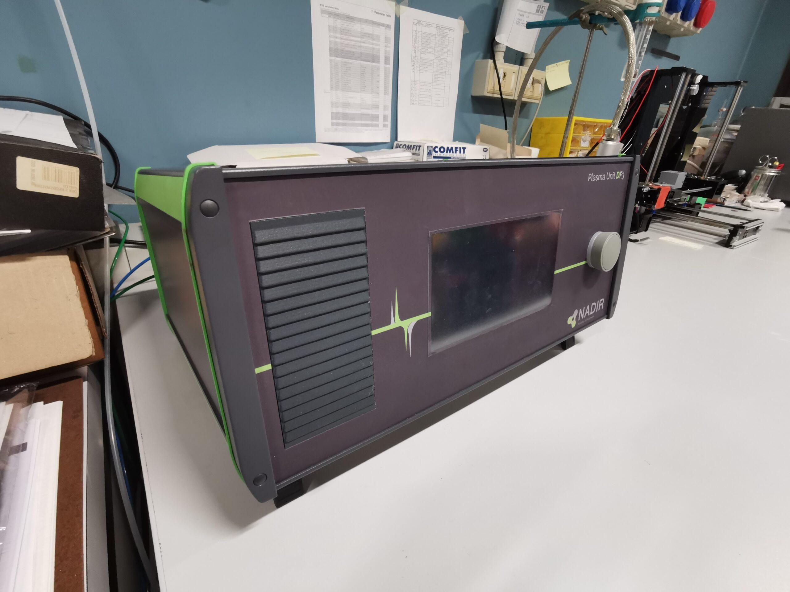
- Dual-frequency atmospheric plasma jet for cold, efficient and clean plasma surface treatments
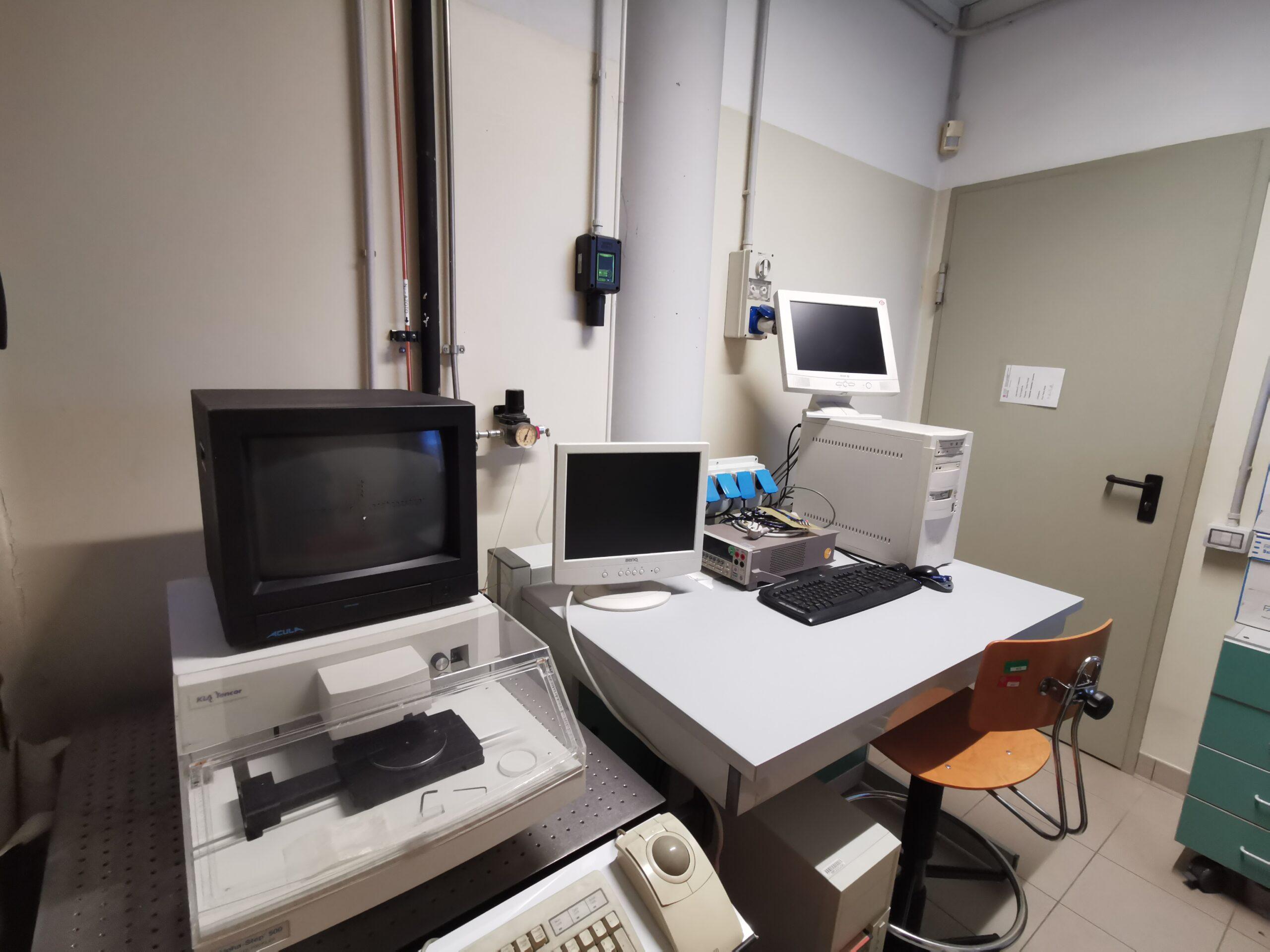
- Alpha-Step profiler for 2D profiling, providing up to 2000 μm vertical range, Ångström resolution, low force (down to 1 mg)


