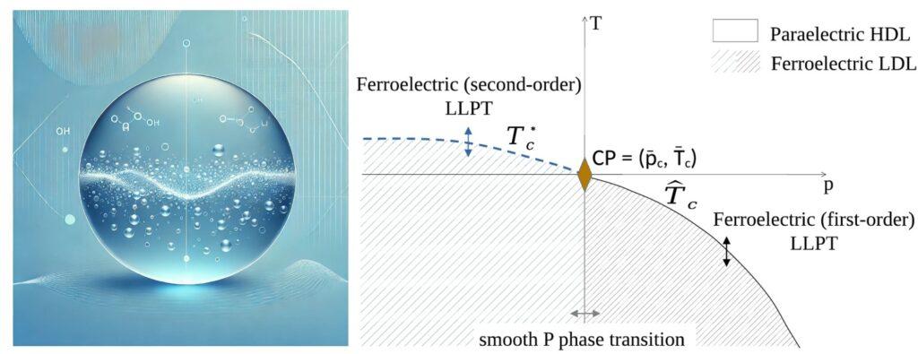
News

Skin-safe, flexible photodetectors combine graphene and carbon dots for wearable sensing

Researchers from Ca’ Foscari University of Venice, working within the SUPERVenice research unit, have developed a new type of flexible, skin-compatible photodetector that can sense light across a broad range of wavelengths while operating at low voltage and remaining safe for direct contact with human skin. The device, reported in Advanced Functional Materials, combines graphene with specially engineered carbon dots on a plastic substrate, creating a lightweight and bendable photodetector suitable for wearable electronics and on-skin sensing applications. Addressing a key challenge in wearable optoelectronics Photodetectors—devices that convert light into electrical signals—are essential components in technologies ranging from cameras and optical communications to medical sensors. Conventional photodetectors, often based on rigid silicon electronics, perform well but are poorly suited for wearable or skin-integrated systems, where flexibility, low power consumption and biocompatibility are crucial. Many flexible photodetectors reported to date compromise on at least one of these requirements. Some offer high sensitivity but rely on toxic materials such as lead- or cadmium-based quantum dots; others are flexible but operate over a narrow spectral range or lack evidence of skin safety. The new work addresses these limitations by combining broadband optical response, mechanical flexibility and verified skin compatibility within a single device architecture. Carbon dots and graphene: complementary roles The photodetector is built by integrating hydrothermally synthesized carbon dots with single-layer graphene transferred onto a polyethylene terephthalate (PET) substrate. The carbon dots act as the light-absorbing element, while graphene provides an efficient, high-mobility pathway for charge transport. Unlike conventional quantum dots, the carbon dots used in this study are metal-free, environmentally benign and inherently biocompatible. By carefully tuning their synthesis conditions, the researchers engineered the dots to absorb light not only in the ultraviolet but also across the visible and near-infrared range, extending roughly from 400 to 800 nanometers. Graphene alone absorbs only a small fraction of incoming light, but when coupled to the carbon dots it efficiently collects photogenerated charge carriers, enabling a measurable electrical response across the full spectral window. Low-voltage operation with a biopolymer gate To control the device electronically, the team used a chitosan–glycerol biopolymer electrolyte as a gate dielectric. Chitosan, derived from natural sources such as chitin, is non-toxic and widely used in biomedical applications. This electrolyte enables strong electrostatic gating at very low operating voltages, with optimal performance reached at around 0.5 V, well below the levels typically required by flexible photodetectors. Under illumination, the device shows a gate-dependent photoresponse that can be tuned between different operating regimes, with peak responsivities of approximately 0.19 A/W at 406 nm, 0.32 A/W at 642 nm, and 0.18 A/W at 785 nm. Performance under bending and repeated use Mechanical flexibility is a key requirement for wearable electronics, and the researchers subjected their devices to extensive bending tests. The photodetectors maintained stable operation at bending radii as small as 0.8 cm and showed no significant degradation after up to 1000 bending cycles. The response times, on the order of one second, are compatible with many wearable sensing applications, including biometric monitoring and environmental light sensing. Demonstrated skin compatibility Beyond electrical and mechanical performance, the study directly addresses skin safety, an aspect often assumed rather than tested in wearable optoelectronics. Using reconstructed human epidermis models and fibroblast cultures, the researchers showed that neither the complete device nor its individual components caused skin irritation or cytotoxic effects. Importantly, illumination under realistic operating conditions did not induce detectable reactive oxygen species (ROS) generation, indicating that the device is photo-safe for on-skin use. Toward practical wearable photonics While the device is presented as a proof of concept, the authors emphasize that the materials and fabrication steps are compatible with scalable, low-cost processing. Future work will focus on improving detectivity, optimizing large-area uniformity, and integrating the photodetectors into functional wearable platforms. By combining metal-free light absorbers, graphene electronics, biopolymer gating and direct biological testing, the study outlines a practical route toward next-generation photodetectors designed from the outset for safe, wearable operation. The full study is published in Advanced Functional Materials and is available at https://doi.org/10.1002/adfm.202523076

Skin-safe, flexible photodetectors combine graphene and carbon dots for wearable sensing Read More »

Simulations Point the Way to Next-Generation SiC Power Packaging

A new study led by researchers at Ca’ Foscari University of Venice, in collaboration with ON Semiconductor, University of Naples Federico II, and University of Applied Sciences Kempten, has unveiled a powerful digital approach to designing the future of high-efficiency power electronics. The work, recently accepted for publication in the IEEE Open Journal of Power Electronics, is titled “Multi-Physics Simulations of a 1.2 kV Embedded SiC Prepackage”. The research team includes Saimir Frroku, Ankit Bhushan Sharma, Pierfrancesco Fadini, Klaus Neumaier, Andrea Irace, Till Huesgen, and Giovanni A. Salvatore, who coordinated the study at Ca’ Foscari’s Department of Molecular Sciences and Nanosystems. A New Era for Power Device Packaging Wide-bandgap (WBG) semiconductors such as silicon carbide (SiC) are transforming power electronics thanks to their ability to operate at higher voltages, temperatures, and switching frequencies than traditional silicon. Yet, packaging remains a critical bottleneck—how these chips are physically mounted, cooled, and electrically connected determines the true performance and reliability of a power module. Embedding the SiC chips directly into an insulating substrate represents a breakthrough approach. By eliminating bulky wire bonds and reducing parasitic inductances, embedded packages enable faster and cleaner switching, boosting efficiency and compactness. However, questions of mechanical reliability and heat management have persisted. Digital Twins for Real-World Reliability The Ca’ Foscari team tackled these challenges through multi-physics finite-element simulations, virtually reconstructing a “prepackage” containing two 1.2 kV SiC MOSFETs and exploring different commercial substrates—alumina, silicon nitride, aluminum nitride, and insulated metal boards (IMS). Their thermomechanical “digital twin” captured how heat and mechanical stress propagate during manufacturing and operation, allowing the team to pinpoint design weaknesses long before physical prototyping. Using a Pareto-based optimization, they identified aluminum nitride (AlN) as the most balanced substrate, achieving a thermal resistance of just 0.27 K/W and low mechanical strain levels. Engineering Smarter Structures The simulations also revealed how to strengthen the package against long-term mechanical fatigue. Replacing the traditional solid copper top contact with a pillar-like interconnect geometry reduced creep strain in the silver sintering layer by up to fourfold—a major leap for reliability. Even the cooling rate during manufacturing proved to be a critical factor: above a certain threshold (around 40 K/min), creep deformation virtually disappears, leaving only reversible plastic strain. This insight offers a new lever for process control and reliability enhancement. Toward Scalable, High-Frequency Power Modules By virtually paralleling four optimized prepackages, the researchers demonstrated a compact power module with only 3 nH of stray inductance, suitable for high-frequency, high-efficiency power conversion—crucial for electric vehicles, renewable-energy systems, and data-center power supplies. “These simulations allow us to accelerate innovation while reducing costly trial-and-error fabrication,” explains Giovanni A. Salvatore, senior author of the study. “Digital modeling provides predictive insights into reliability and performance, helping us design the next generation of power modules that are both efficient and robust.” From Simulation to Sustainable Energy Systems The findings open new perspectives for integrating wide-bandgap semiconductors into compact, thermally stable, and manufacturable modules—an essential step toward electrified mobility and renewable-powered grids. The team’s work exemplifies how virtual engineering and experimental design can converge to drive sustainable innovation in advanced electronics. The full article is available at: https://ieeexplore.ieee.org/document/11224018. All image rights and copyrights are reserved by IEEE.

Simulations Point the Way to Next-Generation SiC Power Packaging Read More »

From Biowaste to Green Electronics: Pioneering Biobased Piezoelectric Films

A team of researchers at the Ca’ Foscari University of Venice has developed a new class of sustainable, flexible, and biodegradable materials that could transform the future of wearable technologies, robotics, and green electronics. The study, published in ACS Nano and featured on its supplementary cover, demonstrates how chitosan-based thin films—derived from crustacean biowaste—can be engineered to achieve record piezoelectric performance. Turning waste into innovation Chitosan, a natural polymer obtained from chitin in crustacean shells, is already known for its biocompatibility and biodegradability. By incorporating chitin nanocrystals into chitosan films, the Ca’ Foscari-led team achieved a twofold increase in piezoelectric response. These soft, transparent films are also stretchable up to 40% strain and exhibit a low Young’s modulus (~100 MPa), closely mimicking the elasticity of human tissues. Why it matters Piezoelectric materials are the backbone of sensors, actuators, and energy harvesters. Today, most commercial devices rely on synthetic polymers like PVDF or inorganic ceramics such as PZT, which raise environmental and health concerns due to their toxicity, rigidity, or reliance on fluorinated compounds. The Ca’ Foscari study shows that biobased materials can achieve competitive performance without compromising sustainability. The films are fully biodegradable, scalable in production, and derived from low-cost biowaste—an example of circular economy applied to advanced materials science. Potential applications Because of their softness and biocompatibility, the new chitosan nanocomposites are particularly suited for: A collaborative effort The research was carried out by the LION group (Laboratory for Innovation in Organic and Nanostructured materials) at Ca’ Foscari’s Department of Molecular Sciences and Nanosystems, in collaboration with international partners. The project received support from EU NextGenerationEU programs (PRIN 2022, iNEST ecosystem) and the PRIMA initiative for sustainable bio-based packaging. Looking ahead According to Giovanni Antonio Salvatore, corresponding author of the study, this work “opens the door to a new generation of sustainable-by-design materials for electronics, capable of replacing polluting polymers and bridging the gap between biological systems and technology.” With this breakthrough, Ca’ Foscari University of Venice further strengthens its position at the intersection of materials science, sustainability, and technological innovation. 👉 Read the full article in ACS Nano: https://doi.org/10.1021/acsnano.4c12855

From Biowaste to Green Electronics: Pioneering Biobased Piezoelectric Films Read More »

Venice shines bright for the FISMAT 2025 conference

From July 6 to 11, 2025, the historic San Giobbe Economics Campus of Ca’ Foscari University welcomed over 1,100 attendees from across the globe for FISMAT 2025, a landmark gathering on the “physics of matter” (eventi.cnism.it). The state‑of‑the‑art venue—with its 23,000 m² dedicated to research, teaching, and relaxation in its lush 2,000 m² garden—offered the perfect backdrop for a conference that exceeded all expectations. The event featured a robust program of invited talks, contributed sessions, and stimulating workshops, including a spotlight on the ISOL technique for medical radionuclide production (LinkedIn). Prominent scientists from institutions like EPFL, Max Planck, Università di Milano, and the Goethe Universität gathered in the Cannaregio district to present cutting-edge research, network, and forge collaborations. Figures of Merit: Attendance: Over 1,100 participants—well beyond initial estimates Speakers: A stellar international lineup, spanning physics, math, and engineering Venue: Conveniently located near Santa Lucia station and Piazzale Roma, with excellent water‑bus connections A Night to Remember: Dinner at Palazzo Moro On Wednesday evening, attendees gathered at the opulent Palazzo Moro, an elegant 16th-century palace nestled in the Cannaregio district. Built by the Moro-Bizio family, this Venetian gem is renowned for its Renaissance façades and frescoed interiors. The palace provided a magical setting for the conference dinner, where guests enjoyed fine Venetian cuisine and heartfelt conversations under shimmering chandeliers. Against the backdrop of historic frescoes, colleagues deepened connections over prosecco, seafood risotto, and local desserts—truly a Venetian feast. What’s Next? With such resounding success, FISMAT 2025 has firmly positioned Venice as a hub for high‑caliber scientific exchange. Attendees departed inspired, carrying with them both fresh insights and unforgettable memories of our city’s magic.   📸 Sneak Peeks from FISMAT 2025 📸 Thank you to everyone—organizers, speakers, sponsors, and attendees—who helped make FISMAT 2025 a shining success. Venice awaits even more groundbreaking discoveries next time!  

Venice shines bright for the FISMAT 2025 conference Read More »

“p-Wave” Magnetism: A Unique Behavior of Electrons

A team led by the Massachusetts Institute of Technology, with the participation of SuperVenice, has recently reported a new form of magnetism, called p-wave, in the material NiI₂. This material exhibits a very peculiar internal magnetic structure: the magnetic moments of the atoms — essentially tiny atomic compasses — are arranged in a spiral pattern. One consequence of this structure is that electrons behave in a unique way: their spins are tied to their energy and direction of motion according to a symmetry known as p-wave. In practice, if an electron reverses its direction of motion, its spin also flips, following precise rules. Furthermore, as demonstrated experimentally, in NiI₂ this property can be controlled electrically, without the need for magnetic fields, which are usually required to manipulate spins.Why it matters Although this type of magnetism in NiI₂ appears only at low temperatures, its potential observation in materials stable at room temperature could lead to the development of much faster and more efficient information processing devices compared to those currently available. The full article, published in the “Nature” journal, is available at the following link: https://www.nature.com/articles/s41586-025-09034-7

“p-Wave” Magnetism: A Unique Behavior of Electrons Read More »

Graphene Meets MoS₂: New Path to Control Light at the Nanoscale

In a study just published in ACS Nano, the team investigated what happens when monolayer MoS₂ — a direct-gap semiconductor just three atoms thick — is stacked with graphene. This combination of two-dimensional (2D) materials reveals a subtle but powerful mechanism: electrical control over light emission without relying on high levels of doping. By carefully tuning the interaction between MoS₂ and graphene, the researchers observed a dramatic suppression of photoluminescence (light emission) from specific exciton species (bound electron-hole pairs), depending on whether the material was isolated or part of a stacked heterostructure. The introduction of graphene changes the game: it enables efficient, voltage-controlled charge transfer, preventing the accumulation of excess carriers in MoS₂ and thus keeping the optical response stable and predictable. The most striking insight? In pristine MoS₂, high doping leads to a superlinear increase in light emission — a kind of optical “amplification” that stops once the system is saturated. This effect disappears completely in the MoS₂/graphene stack, showing that graphene acts as a natural “exciton regulator,” draining away excess charge and suppressing this nonlinearity. Even B-type excitons — typically unaffected by doping due to their ultrafast decay — are modulated by this setup, revealing that charge transfer occurs before excitons can recombine internally. This suggests the presence of a hot-electron transfer channel, a new dimension to 2D material photophysics. Why it matters This work opens the door to more precise control over how atomically thin materials emit light, essential for developing efficient LEDs, photodetectors, and quantum light sources. The use of layered 2D materials to achieve such control, without chemical treatment or structural modification, marks a significant leap forward in optoelectronics and nanophotonics. The SUPERVenice perspective This discovery strengthens Venice’s growing role in frontier materials research. The participation of Ca’ Foscari University through Prof. Domenico De Fazio, member of SUPERVenice, highlights the impact of collaborative, interdisciplinary science rooted in fundamental physics with clear technological implications. The full paper, “Tunable Exciton Modulation and Efficient Charge Transfer in MoS₂/Graphene van der Waals Heterostructures”, is available open-access in ACS Nano. 🔬 Read the paper: ACS Nano DOI

Graphene Meets MoS₂: New Path to Control Light at the Nanoscale Read More »

Securing the Future: A Review of Key Management in QKD Networks

Secure communication is essential to modern digital infrastructure, enabling safe data exchange across global telecommunication networks. As computational capabilities grow, so do threats to classical encryption, prompting the development of advanced cryptographic methods. Quantum Key Distribution (QKD) offers a groundbreaking solution by enabling information-theoretically secure (ITS) key exchange, rooted in the principles of quantum mechanics rather than computational hardness. Unlike traditional methods, QKD remains secure even against adversaries with unlimited processing power. To overcome the distance limitations of direct quantum communication, trusted relay QKD networks have been developed. These networks act as secure extensions to classical systems, facilitating the generation and distribution of cryptographic keys across larger scales. However, due to limited key generation rates, efficient key management is critical, especially when integrating QKD into critical infrastructures. Key management ensures optimal use of resources, addressing challenges like key allocation, storage, and prioritization. The accepted work addresses this need by providing a comprehensive review of key management approaches tailored for trusted-relay QKD networks. The surveyed strategies encompass various aspects of key lifecycle management, such as key generation, storage, routing, prioritization, and expiration, as well as integration with existing security protocols and infrastructure requirements. Through in-depth analysis, the paper aims to identify promising techniques, highlight existing limitations, and outline areas for further research. The ultimate goal is to facilitate the strategic development and deployment of scalable, secure, and efficient QKD networks that can be seamlessly integrated into existing communication infrastructures, paving the way for a quantum-safe future. The work is also the result of a long-term research cooperation between researchers from University of Sarajevo (Department of Telecommunications) Bosnia-Erzegovina, VSB-Technical University of Ostrava (Department of Telecommunications) Czech Republic and Ca’ Foscari University of Venice (Department of Molecular Sciences and Nanosystems) Italy. The full article is available at the following link: https://dl.acm.org/doi/10.1145/3730575

Securing the Future: A Review of Key Management in QKD Networks Read More »

Introducing the Ferro-Power MOSFET

Power MOSFETs are key to modern electronics, enabling efficient power conversion and control in a wide range of applications.  However handling short-circuit events remains a challenge—especially for SiC and GaN devices. The Ferro-Power MOSFET changes the game by integrating ferroelectric materials into the gate, reducing temperature rise and enhancing reliability without modifying the device layout or control electronics. Simulations of a 1.2 kV SiC MOSFET show up to 31% lower temperatures and 42% less current surge during faults, making this a breakthrough for automotive and industrial power systems. With advances in CMOS-compatible hafnium oxide, this innovation is set to shape the future of power semiconductors! #PowerElectronics #MOSFET #SiC #GaN #Innovation #TechBreakthrough #Ferroelectrics #Hafnium Oxide   Check out our paper (in collaboration with Prof. A. Irace and L. Maresca from UniNa):  The Ferro-Power MOSFET: Enhancing Short-circuit Robustness in Power Switches with a Ferroelectric Gate Stack

Introducing the Ferro-Power MOSFET Read More »

Wigner crystal for elongated colloids observed and explained

In 1934 Nobel Prize winner Eugene Wigner predicted the existence of a crystal formed by electrons at low density stabilized by strong electrostatic repulsions. Up to date, this crystal has never been observed. However, it was observed experimentally and explained theoretically in the realm of spherical colloids, nanoparticles with nanometric sizes, and nearly perfect spherical shapes. By contrast, the common belief was that this was not observable for rod-like colloidal particles with a high aspect ratio. This recent study, originating from a collaboration from the experimental group of the CNRS in Bordeaux with a theoretical group at Ca’ Foscari University of Venice led by Prof. Achille Giacometti, showed otherwise. At low density and strong electrostatic repulsions, a solution of nearly monodisperse rod-like colloidal particles tends to form a crystal structure stabilized by a combined minimization of the electrostatic potential and the maximization of the entropy associated with the longitudinal and transversal fluctuation of the particles. This has been unambiguously observed experimentally and supported by numerical simulations. Figure (Left): Two charged rods in water and counterions. Figure (Right): Different liquid crystal phases numerically observed for aspect ratio L/D =10 and different Debye wave number kD (WCA= kD → ∞) The full article is available at the following link: https://journals.aps.org/prl/abstract/10.1103/PhysRevLett.134.118101

Wigner crystal for elongated colloids observed and explained Read More »

SUPERVenice Shines at Orientation Event

On January 17, 2025, SUPERVenice, the group of engineering and physics innovators, left a lasting impression at the sixth edition of Professione Scienziate. Held at the Alfa Building on the Ca’ Foscari Science Campus in Venice, the event was a platform to showcase the fascinating and practical aspects of STEM fields to high school students from across the region. This year’s event was particularly successful, with SUPERVenice captivating hundreds of visitors with their engaging and hands-on demonstrations. The SUPERVenice stand drew significant attention, showcasing a range of interactive experiments designed to inspire and educate. Among the highlights: The SUPERVenice team’s innovative approach drew large crowds throughout the event, with students and teachers alike praising the accessibility and excitement of the presentations. Beyond simply entertaining, these demonstrations effectively communicated the practical and transformative power of engineering physics, igniting interest among students who are now considering enrolling in the bachelor’s and master’s programs in Engineering Physics at Ca’ Foscari. The event marked a significant milestone in the orientation efforts aimed at encouraging high school students to pursue STEM careers. SUPERVenice’s ability to bridge complex scientific concepts with engaging and relatable demonstrations solidified its reputation as a leader in fostering the next generation of engineers and physicists. As the enthusiasm from Professione Scienziate fades into memory, SUPERVenice looks forward to welcoming these inspired students to its programs, where they will embark on a journey of discovery and innovation. Event Link: https://www.unive.it/data/agenda/6/96921

SUPERVenice Shines at Orientation Event Read More »